
Foundational Circuit Board Design Principles for Reliable Printing Machine Operation
Design for Manufacturability (DFM) and Design Rule Checking (DRC) in Printing Machine Circuit Board Production
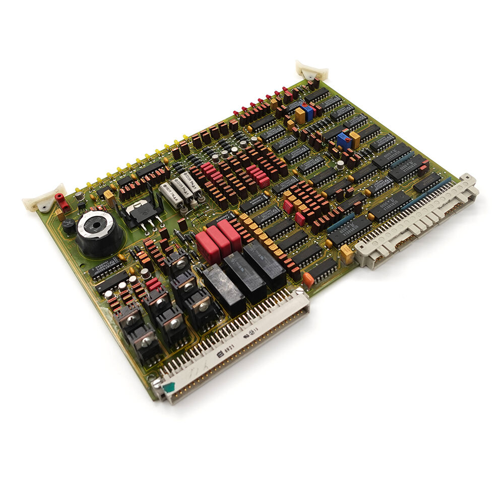
Design for Manufacturability (DFM) ensures printing machine circuit boards meet rigorous production requirements while minimizing cost and time-to-market. Core strategies include reducing component count, optimizing part geometry for automated placement, and specifying realistic tolerances that align performance goals with fabrication capabilities—cutting material waste by up to 30% in complex layouts and shortening manufacturing cycles. Complementary Design Rule Checking (DRC) automates verification of trace widths, spacing, and via placement against IPC-2221 standards, flagging unmanufacturable features before fabrication. This is especially critical for high-density control boards, where even minor layout deviations can degrade motion accuracy and increase registration errors.
Gerber File Accuracy, CAD-to-PCB Integration, and Fabrication Yield Impact
Gerber file fidelity directly determines circuit board quality and yield in printing machine production. Minor misalignments or aperture definition errors can cause etching defects in high-speed data paths—compromising print head synchronization and media transport timing. Seamless CAD-to-fabrication data transfer eliminates interpretation errors responsible for 62% of first-article failures. Manufacturers achieving 99.5% Gerber accuracy report 40% fewer solder mask registration issues and 25% higher assembly throughput. Robust integration preserves impedance-controlled routing and thermal relief patterns from design intent to physical board—ensuring consistent print head responsiveness and long-term media handling reliability.
Circuit Board Performance Drivers: Signal Integrity, Thermal Control, and Layout Precision
High-Speed Trace Routing and Component Placement for Stable Print Control Systems
Signal integrity is foundational to stable print control. High-speed digital traces must be carefully routed to minimize electromagnetic interference—particularly by isolating them from analog sensors, power supplies, and motor drivers. Impedance matching preserves waveform fidelity across transmission lines, while strategic component placement reduces parasitic capacitance and inductance, shortening signal paths and eliminating latency-induced jitter. Poor routing can introduce reflections that degrade print head positioning accuracy by up to 15%. To maintain noise immunity in compact, densely packed designs, engineers prioritize uninterrupted ground planes and differential pair routing—especially for encoder feedback and real-time motion control signals.
Thermal Management Strategies and Solder Mask Application Methods for Long-Term Circuit Board Reliability
Continuous operation in industrial printing environments demands proactive thermal management. Copper weight selection (e.g., 2oz vs. 4oz) balances current-carrying capacity with thermal conductivity, while arrays of thermal vias efficiently channel heat from power components—such as stepper motor drivers and LED print head arrays—to heatsinks or chassis surfaces. Solder mask application serves dual roles: preventing solder bridging during reflow and shielding traces from moisture, dust, and chemical exposure common in ink-rich environments. CTE mismatch between FR4 substrates and copper traces creates mechanical stress during thermal cycling; mitigation includes using high-Tg laminates (>170°C), epoxy-based solder masks with ≥80% coverage, and evenly distributed thermal masses to avoid localized hotspots. Proper thermal profiling during assembly prevents micro-cracks in solder joints—extending board service life by 30% in demanding industrial settings.
Industrial-Grade Circuit Board Reliability: Standards, Environment, and Durability
IPC Class 2 vs. Class 3 Compliance for Harsh, Space-Constrained Printing Environments
IPC classification dictates circuit board suitability for specific operational environments—and for industrial printing machinery, Class 3 compliance is non-negotiable. While Class 2 boards tolerate minor cosmetic flaws and are appropriate for consumer-grade printers, Class 3 certification enforces zero-tolerance defect limits essential for equipment operating under vibration, wide temperature swings (>30°C ambient variation), and airborne particulate contamination. Key distinctions include:
- Zero allowable reduction in annular rings, unlike Class 2’s permitted 50% reduction
- Tighter electrical testing margins: ≤1% impedance variation versus Class 2’s ≤5%
- Extended thermal cycling validation: minimum 500 cycles from –40°C to 125°C (Class 2: 100 cycles)
| Feature | IPC Class 2 | IPC Class 3 |
|---|---|---|
| Target Environment | Controlled | Harsh Industrial |
| Permitted Annular Ring | 50% reduction allowed | Zero reduction permitted |
| Thermal Stress Cycles | 100 cycles certification | 500 cycles minimum |
Class 3 boards undergo mandatory solder joint inspections and microsectional analysis—critical for space-constrained chassis where field repair is impractical. This level of scrutiny reduces latent field failures by 40%, supporting uninterrupted, high-uptime printing operations.
Optimizing Circuit Board Design for Cost, Complexity, and Scalable Manufacturing
Subtractive, Additive, and Semi-Additive Processes in High-Density Printing Machine Circuit Board Fabrication
Fabrication process selection shapes performance, scalability, and cost in high-density printing machine boards. Subtractive methods—etching copper from laminated substrates—remain dominant for high-volume production due to maturity and cost efficiency, though they impose practical limits on trace density and minimum feature size. Additive techniques electroplate conductive patterns directly onto dielectric layers, enabling sub-25µm traces and reducing material waste by 30–40%, making them ideal for low-volume prototyping and ultra-dense interconnects. Semi-additive manufacturing (SAM) combines both: a thin copper seed layer is patterned and selectively plated, achieving micron-scale resolution, excellent impedance control, and superior compatibility with embedded passives and thermal expansion management. For industrial printing systems requiring HDI architecture, embedded components, or stringent signal integrity, SAM delivers optimal balance—supporting scalable transition from prototype to volume production without compromising reliability.
FAQs
What is the purpose of Design for Manufacturability (DFM) in circuit board production?
DFM ensures circuit boards are designed to meet strict production standards while minimizing fabrication costs and time-to-market. It involves optimizing component placement, part geometries, and tolerance specifications.
How does Gerber file accuracy influence circuit board manufacturing?
Gerber file fidelity directly impacts circuit board quality. Accurate Gerber files reduce errors such as etching defects and solder mask misalignments, improving overall manufacturing yield and efficiency.
What is the difference between IPC Class 2 and Class 3 standards?
Class 2 is suitable for controlled environments and allows some flaws, while Class 3 demands higher reliability, zero defect tolerance, and extended thermal cycling for harsh industrial settings.
Why is thermal management important for circuit boards in printing machines?
Proper thermal management extends circuit board lifespan and prevents thermal stress-related failures, especially under continuous operation in high-demand industrial environments.
What are the advantages of semi-additive manufacturing (SAM) for circuit boards?
SAM enables high-density designs with micron-scale resolution while maintaining excellent impedance control and compatibility with embedded components, making it ideal for transitioning from prototypes to volume production.
Table of Contents
- Foundational Circuit Board Design Principles for Reliable Printing Machine Operation
- Circuit Board Performance Drivers: Signal Integrity, Thermal Control, and Layout Precision
- Industrial-Grade Circuit Board Reliability: Standards, Environment, and Durability
- Optimizing Circuit Board Design for Cost, Complexity, and Scalable Manufacturing
-
FAQs
- What is the purpose of Design for Manufacturability (DFM) in circuit board production?
- How does Gerber file accuracy influence circuit board manufacturing?
- What is the difference between IPC Class 2 and Class 3 standards?
- Why is thermal management important for circuit boards in printing machines?
- What are the advantages of semi-additive manufacturing (SAM) for circuit boards?